
The Silicon Horizon: Tapping into the Job Boom Driven by India’s Semiconductor Push
The Scale of the Opportunity
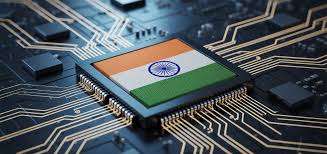
The global semiconductor supply chain is undergoing a seismic shift, and India is positioning itself as a pivotal player. Fueled by ambitious government incentives like the India Semiconductor Mission (ISM) and major investments from global giants like Micron and Tata, the country is transitioning from being primarily a design hub to an end-to-end manufacturing powerhouse. This monumental shift is not just about economic self-reliance; it is triggering a massive job creation wave, projected to reach up to one million jobs by 2026 across the value chain.
However, this isn’t a volume-hiring spree for generalized engineering roles. The semiconductor industry demands specialized, niche expertise, and understanding where the current and future skill gaps lie is crucial for students, professionals, and academic institutions alike.
The New Ecosystem: From Design to Fabrication (Fab) and Packaging (ATMP)
India’s growth strategy smartly targets three core segments of the value chain, each creating distinct sets of job roles:
1. Advanced Design (VLSI)
India has long been recognized for its prowess in Very Large Scale Integration (VLSI) design, contributing nearly 20% of the world’s design workforce. While core design continues to grow, the focus is now on more sophisticated, application-specific roles:
- RTL Design and Verification Engineers: Responsible for creating and validating the digital logic of the chip using Hardware Description Languages (like Verilog and SystemVerilog).
- Physical Design Engineers: The “backend” specialists who translate the logical design into a physical layout (floorplanning, placing, routing) ready for manufacturing. Expertise in tools like Synopsys ICC2 or Cadence Innovus is essential.
- Analog & Mixed-Signal Design Engineers: Crucial for designing components like ADCs and PLLs that bridge the digital world with real-world signals.
2. Fabrication (Fab) and Process Engineering
The most complex and capital-intensive part of chip-making, Fab operations require deeply specialized skills to manage the extreme precision and cleanroom environments.
- Process Engineers: These experts optimize every step of the fabrication, including photolithography, etching, and Chemical Mechanical Planarization (CMP), to maximize manufacturing yield.
- Equipment Maintenance Technicians: High-stakes roles focused on operating, calibrating, and troubleshooting ultra-sensitive manufacturing machinery in cleanroom environments.
- Materials Scientists: Focusing on the specialty chemicals, gases, and materials required for wafer production.
3. Assembly, Testing, Marking, and Packaging (ATMP/OSAT)
With major projects like the Micron ATMP plant in Gujarat, roles focusing on post-fabrication quality assurance are spiking.
- Semiconductor Packaging Engineers: Specializing in advanced techniques like Flip-chip, BGA, and 3D chiplet integration to ensure chips are reliably assembled.
- Test and Validation Engineers: Developing and running rigorous tests (often using Automated Test Equipment, or ATE) to confirm chip reliability and performance before they ship to customers.
The Niche Skills Driving Demand
The common thread across all these roles is a move toward high-value, specialized expertise. Companies are prioritizing quality over quantity in their hiring, with demand for niche skills driving nearly half of all openings in design centers.
Beyond foundational knowledge in Electrical Engineering and Semiconductor Physics, the most critical niche skills include:
| Skill Domain | Specific Technical Competency | Importance |
|---|---|---|
| VLSI/Design | Proficiency in SystemVerilog, UVM (Universal Verification Methodology), and advanced Electronic Design Automation (EDA) tool flows. | High |
| Manufacturing | Expertise in Cleanroom Protocols, Metrology, Yield Analysis, and statistical process control (SPC). | Critical |
| Advanced Packaging | Knowledge of chiplet architecture, 2.5D/3D integration, and materials science for thermal management. | Emerging |
| Emerging Tech | Experience with AI/ML hardware acceleration, specialized architecture like RISC-V, and developing firmware for embedded systems. | Future-Proofing |
Bridging the Talent Gap
While India possesses a vast talent pool, the unique manufacturing and process engineering skills required for Fab and ATMP operations currently face a significant gap. To bridge this, academia and industry are collaborating closely. Initiatives like the specialized Delta Class programs, Marvell’s research facility partnerships with IITs, and industry-tailored embedded design courses are ensuring that students gain hands-on training and exposure to industry-standard tools before they graduate.
The semiconductor surge offers a profound opportunity for India’s engineering talent. It demands commitment to continuous learning and a willingness to dive deep into highly technical domains. For those ready to master the intricacies of silicon, the future in India’s high-tech landscape is exceptionally bright.